1. Validation status
These instructions apply to custom I/O PCB v1.2, the current tested board.
2. Safety notice
- Use a soldering iron stand and work in a ventilated area.
- Use a fume extractor.
- Take appropriate precautions when working with leaded solder.
- Wear eye protection when trimming component leads.
- Observe antistatic precautions.
- Disconnect USB power and the battery during assembly and continuity tests.
- Do not install a non-rechargeable CR2032 until the RTC module’s charging resistor has been removed or otherwise disabled.
3. Required parts and tools
See Parts list and Skills and tools.
Use the latest supported PCB revision (v1.2 at this time). Download the v1.2 fabrication files from the Morse Scout hardware repository on GitHub.
4. Procedure
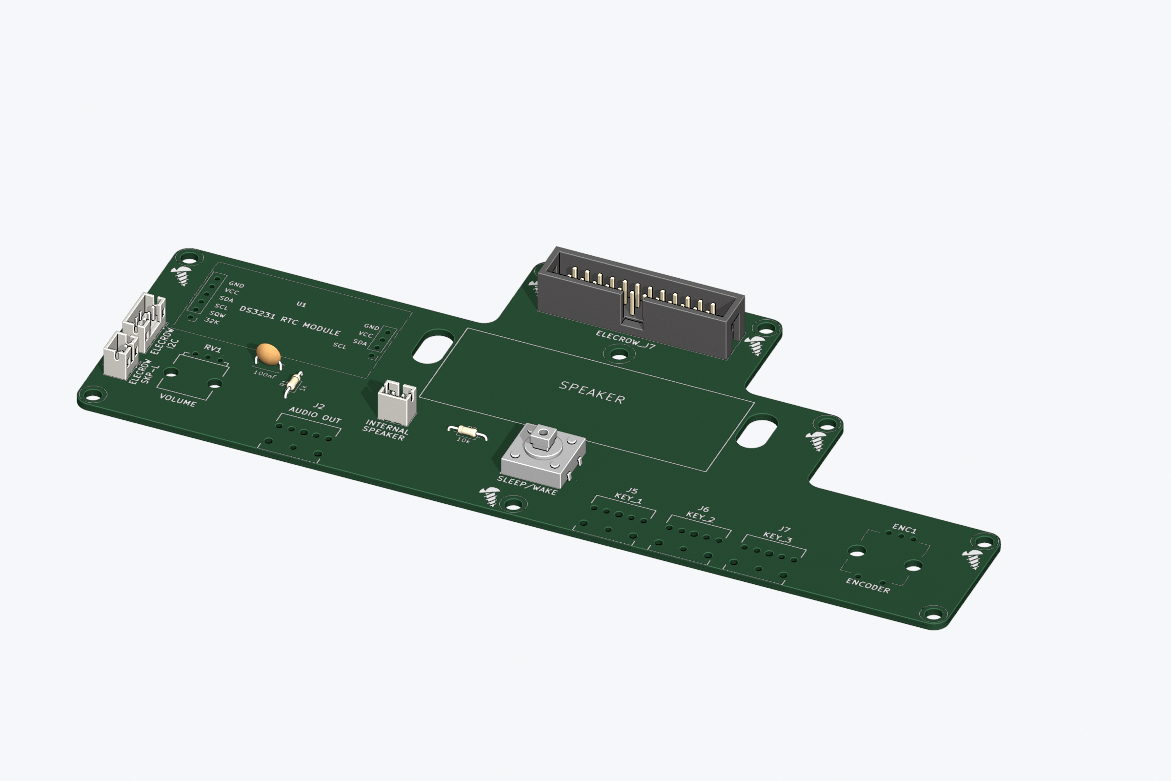
- Inspect the bare PCB for damaged plating and shorts. Confirm board revision, it is printed on the back of the board.
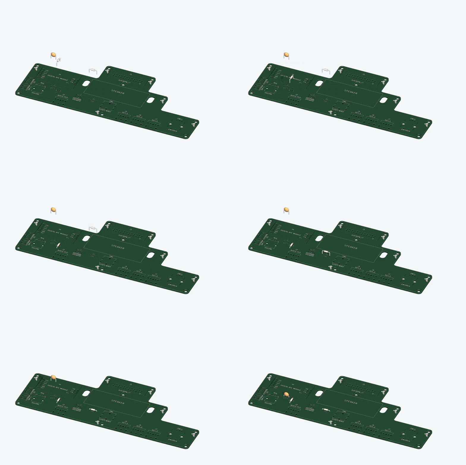
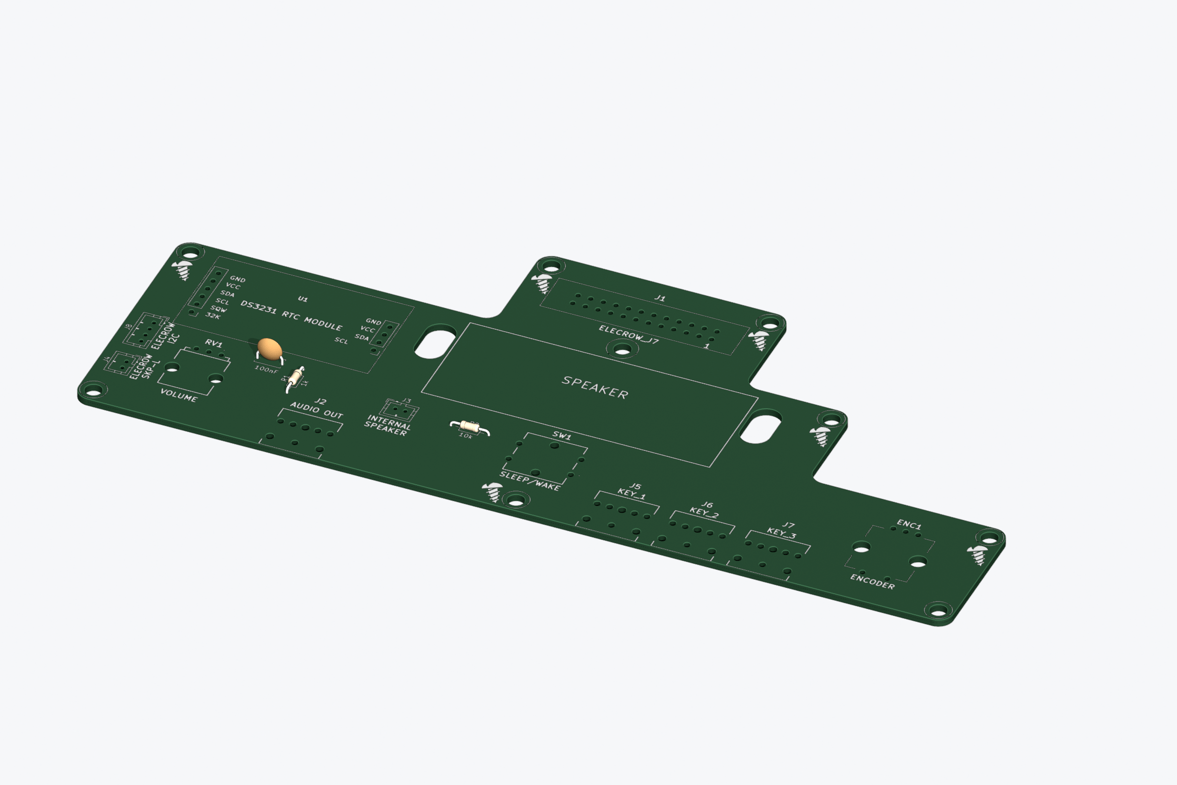
- Fit resistors
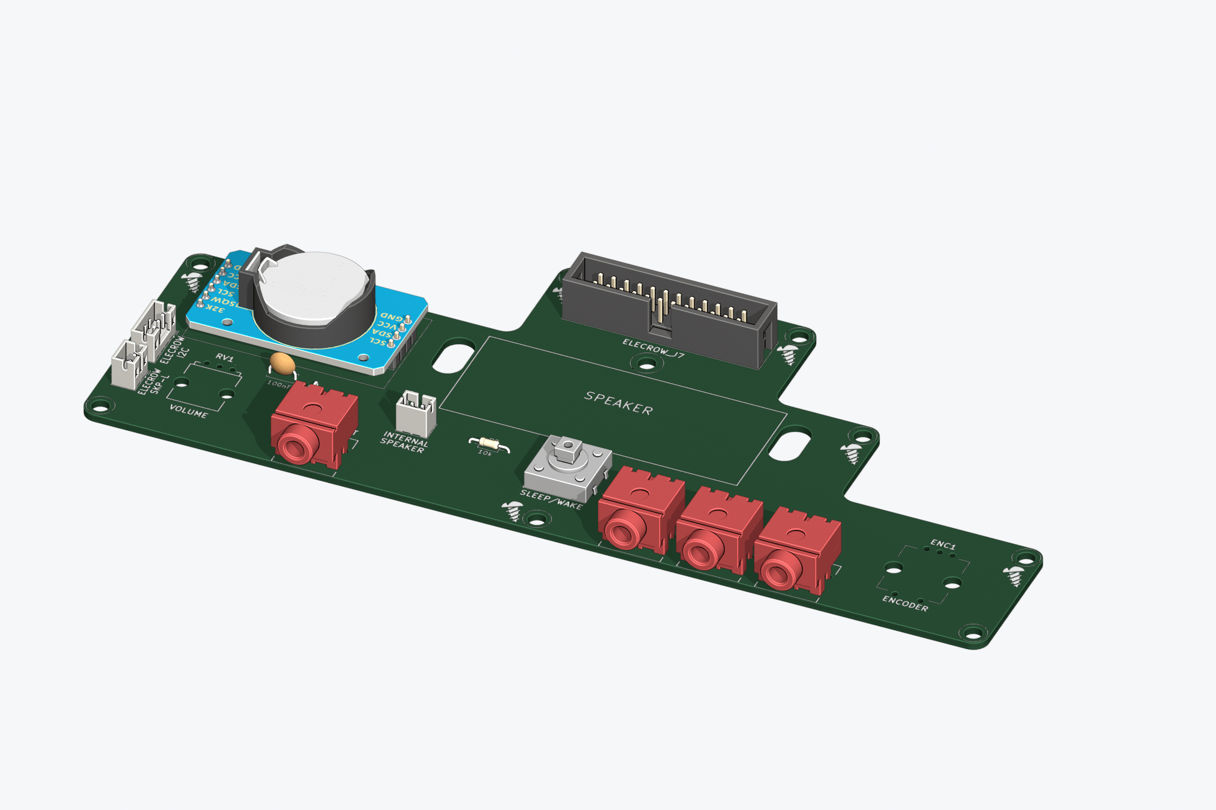
R1andR2and capacitorC1. Solder them in place, then trim their leads. The silkscreen identifies the resistor values: 1 kΩ forR1and 10 kΩ forR2.
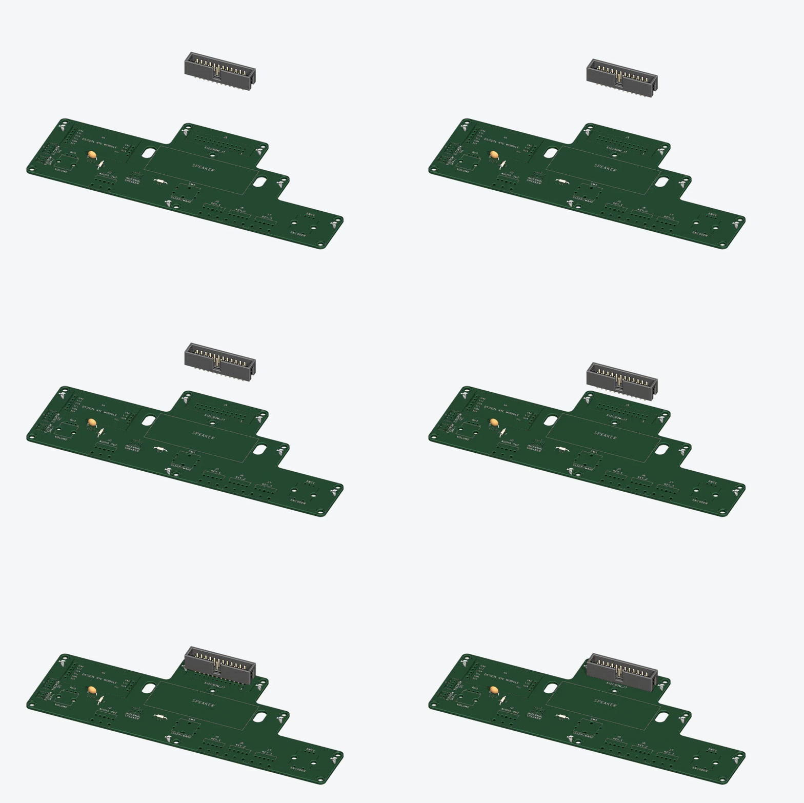
- Fit the 24-pin
J1connector and solder it in place. The connector can be fitted with the notch facing either direction, but installing it with the notch facing forward provides a consistent orientation.

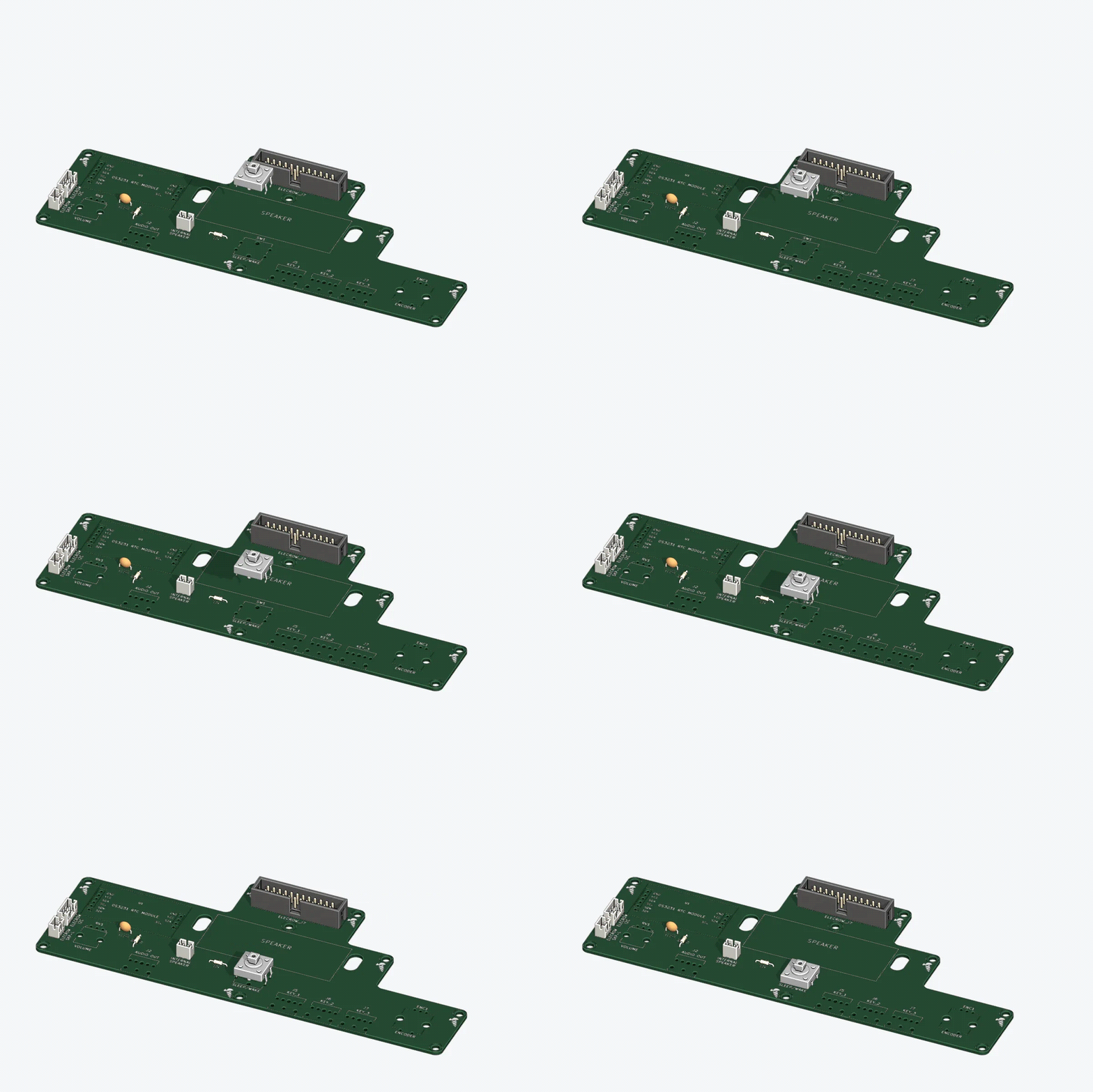
- Fit
J3,J4, andJ8, checking pin 1 and the latch orientation. TheJ8latch should be on the right side of the socket, facing the potentiometer.


- Fit the Sleep/Wake button,
SW1. Align pin 1 with the square pad at the lower-right corner of the footprint.
- Fit the four 3.5 mm jacks:
J2andJ5throughJ7. Their bodies deliberately extend beyond the PCB edge. Solder the center ground pin first, and confirm that each jack sits flat against the board before soldering its remaining pins.


- Prepare the DS3231 module before installing it on the I/O PCB. Remove
resistor
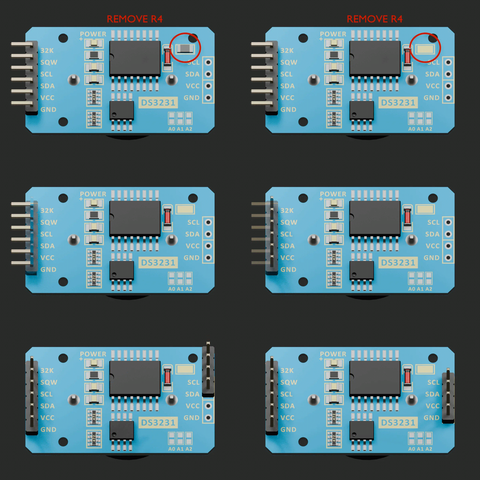
R4to disable the integrated coin-cell charging circuit before fitting a non-rechargeable CR2032. The charging circuit is designed for a 5 V supply, but Morse Scout powers the module at 3.3 V. Charging may not work correctly at that voltage, and the circuit must not remain connected to a non-rechargeable cell. The module comes with a six-pin right-angle header. Carefully straighten its pins and trim the excess length, then fit the required four-pin header.
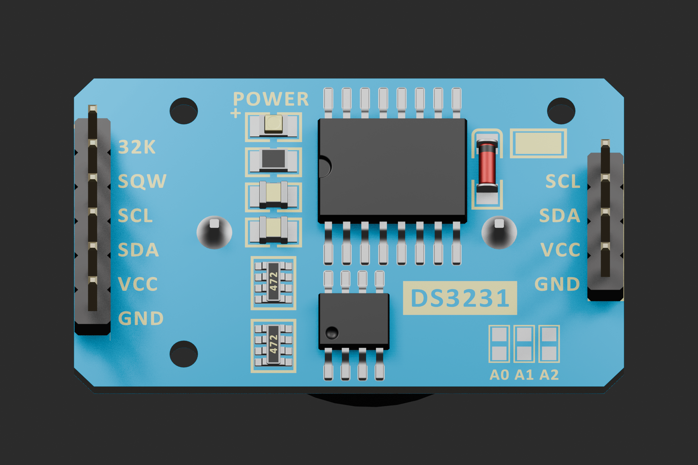
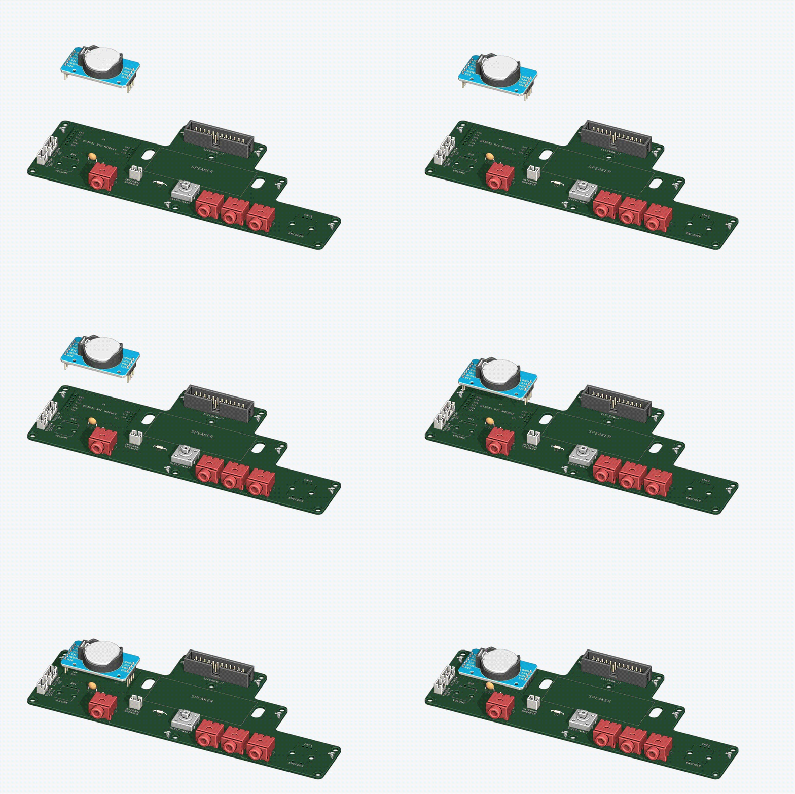
After preparation is complete, install the RTC module on the I/O PCB. You can solder both headers directly to the I/O board or use sockets so the module remains removable.
- Install
RV1andENC1last. Confirm that both controls sit squarely against the board and that their shafts are vertical. Their long shafts amplify even a small alignment error. Solder one ground pin first, align the potentiometer or encoder while reheating that joint if necessary, and then solder the remaining pins.


- Clean and visually inspect every joint. Check for bridges around the dense jack and encoder pins.
5. Expected result
A fully assembled v1.2 board with straight connectors and controls and no solder bridges.

6. Inspection or test
With all power disconnected:
- Check resistance between
3V3andGNDfor an accidental short.

- Check J1 pin 1 orientation.
- Check the J8 latch orientation; it should be on the right side of the connector.
- Check continuity for the J1 mappings in Build troubleshooting.
After these checks pass, connect the display board and complete Bring-up tests.
7. Failure conditions
- Wrong J8 orientation.
- Solder bridges or open joints.
- The RTC module’s charging circuit remains active and attempts to charge a non-rechargeable CR2032 battery.